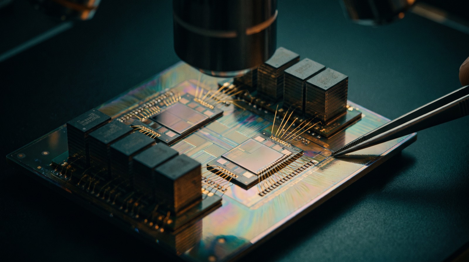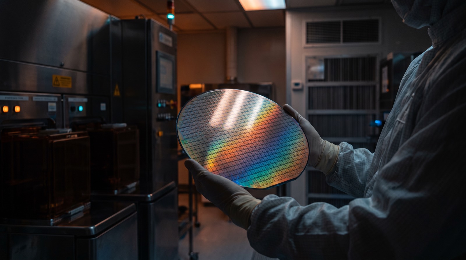
An B200 begins as quartz sand and ends as 208 billion transistors. The path between is the most precise manufacturing humans do.
Wafers
Silicon is refined to 99.9999999% purity, grown into a single crystal ingot, and sliced into 300 mm wafers polished to atomic flatness. Each wafer will carry dozens of GPU-sized dies — or, for Cerebras, exactly one chip the size of the wafer.
Printing with impossible light
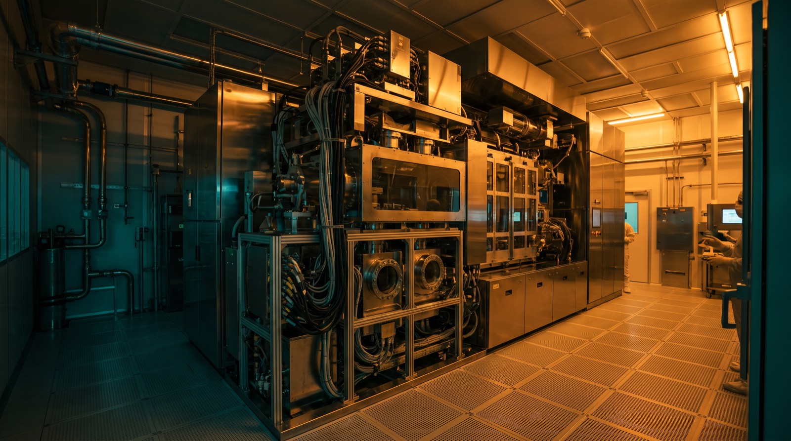
Chips are built layer by layer — dozens of them — by photolithography: coat the wafer with light-sensitive resist, project the circuit pattern, etch, deposit material, repeat. Feature sizes below ~7 nm require EUV light at 13.5 nm wavelength, produced by vaporizing tin droplets with lasers 50,000 times a second and steered by mirrors flat to fractions of an atom. Exactly one company on Earth — ASML — can build these machines, at ~$180M each (High-NA: ~$380M). That monopoly is the deepest chokepoint in this entire database.
Transistors, then wiring
The front end builds the transistors — now 3D fins (FinFET) giving way to gate-all-around nanosheets at 2 nm. The back end wires them with 15+ layers of copper interconnect. Any speck of dust ruins a die, so it all happens in cleanrooms thousands of times cleaner than an operating theater, run by Applied Materials, Lam, TEL and KLA tools.
Yield: the economics hidden in defects
Defects scatter randomly, so the bigger the die, the worse the odds every part of it is perfect. That is why an 814 mm² reticle-limit GPU is expensive — and why the industry moved to chiplets: small dies yield well, and packaging joins them. A wafer takes 3–4 months and thousands of steps; a leading-edge fab costs $20–30B, which is why only TSMC, Samsung and Intel still play.
Package and test
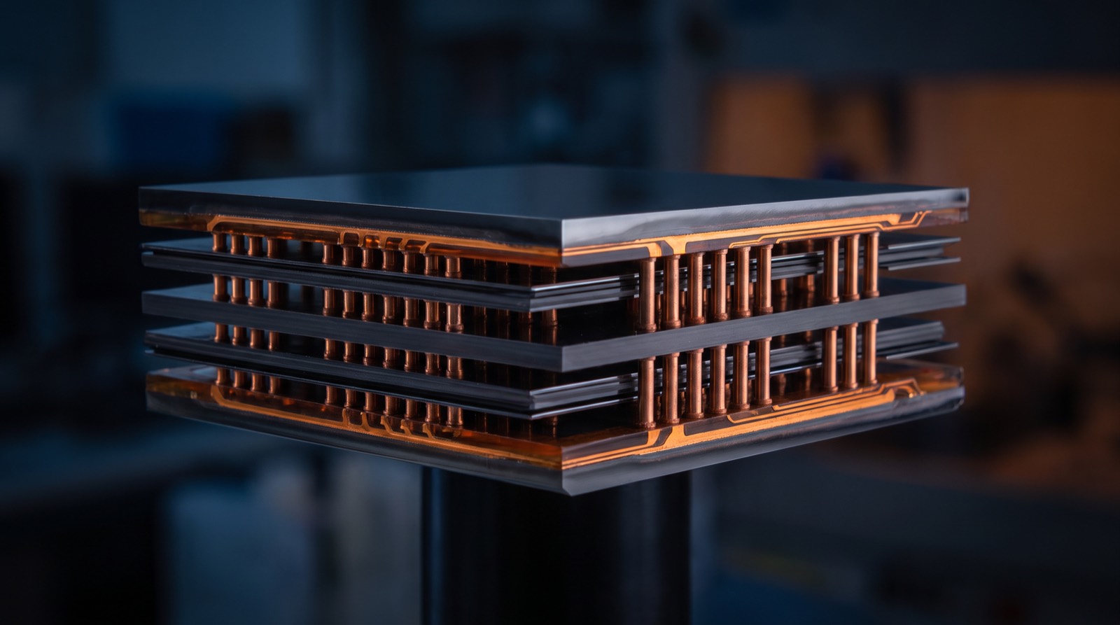
Finished dies are cut out (DISCO saws), stacked with HBM on interposers (CoWoS), tested, binned and mounted. Packaging — once an afterthought — is now a bottleneck chapter of its own: see Advanced Packaging.
The point
Every layer of this process is a monopoly or near-monopoly — one lithography vendor, one dominant foundry, three memory makers, a handful of toolmakers. AI's supply chain is not a market so much as a chain of single points of failure, which is why governments now treat it as strategic terrain (the chip war).
 2
2