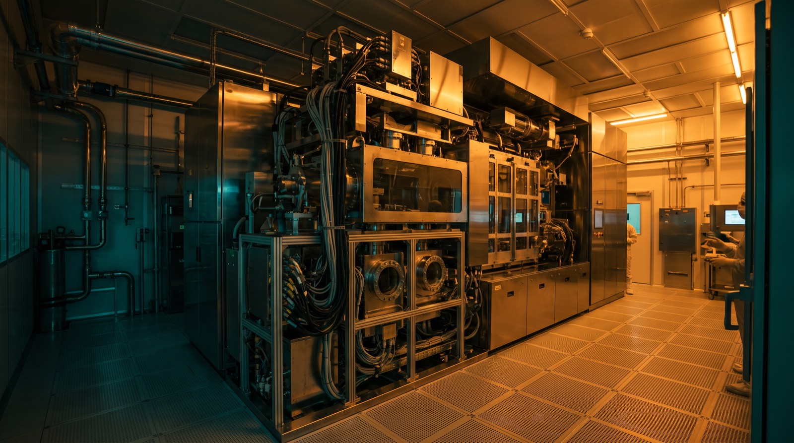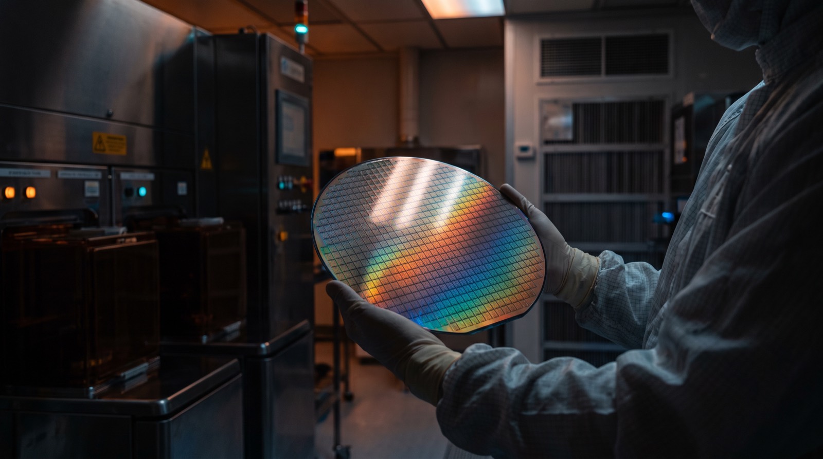
In 2023–24 the world's GPU supply was not limited by wafers, EUV machines or even HBM — it was limited by an assembly step most people had never heard of: CoWoS.
Why packaging suddenly matters
Two forces collided. First, classic scaling slowed — you can no longer just shrink transistors for free performance. Second, dies hit the reticle limit: lithography machines cannot print larger than ~858 mm², and H100 was already there. The escape route is horizontal and vertical: put multiple dies in one package and wire them as if they were one chip. The package became the product.
2.5D: CoWoS and friends
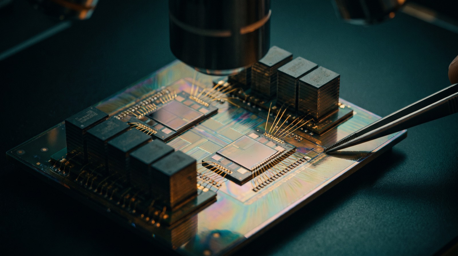
Chip-on-Wafer-on-Substrate places GPU dies and HBM stacks side by side on a silicon interposer — a wiring layer with connections far denser than any circuit board. Every NVIDIA and AMD flagship uses it. Capacity is measured in wafer starts per month, and TSMC has multiplied it several-fold since 2023, with Amkor and ASE adding overflow capacity. CoWoS-L — silicon bridges embedded in an organic interposer — carries Blackwell's two-die assemblies and Rubin's larger ones.
3D: true stacking
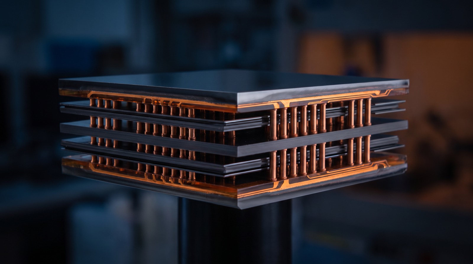
Hybrid bonding joins dies face-to-face with copper pads at micron pitch — no solder bumps, near-monolithic bandwidth. AMD's MI300 stacks compute dies on base dies this way; HBM4's base dies and future GPUs push it further. Toolmakers Besi and Applied Materials own this niche.
Chiplets: the design philosophy
Chiplets split a processor into small dies that yield well, mix process nodes (compute on N3, I/O on cheaper N6), and scale past the reticle. AMD proved it in CPUs and MI300; NVIDIA joined with Blackwell's two dies; UCIe aims to standardize die-to-die links across vendors.
The strategic read
Packaging is now roadmap-limiting: Blackwell's early 2024 delay was a packaging revision; CoWoS allocation defines who ships GPUs; US subsidies fund domestic packaging precisely because a fab without advanced packaging is only half a supply chain. Watch CoWoS capacity numbers the way older analysts watched wafer starts.
 4
4