Раздел базы данных · 26 записи
Foundry и упаковка
Where the chips are actually made: leading-edge process nodes, advanced packaging, and the equipment monopolies underneath.
Заметки с места событий
Всё, что выше этого уровня, — проектирование; здесь атомы действительно перемещаются. Это также самое концентрированное место в мировой экономике: одна компания производит почти каждый передовой ИИ-чип, используя машины, которые умеет строить лишь одна другая компания.
Начните с этих трёх
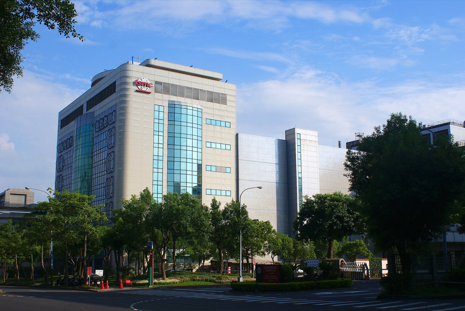 TSMC
Незаменимая компания. Почти каждый чип в этой базе данных рождён здесь.
EL
EUV Lithography
Машина, которую умеет строить только ASML, — капли олова, лазеры и самые плоские зеркала из когда-либо созданных.
CO
CoWoS
Этап корпусировки, который держал мировые поставки GPU в дефиците два года.
TSMC
Незаменимая компания. Почти каждый чип в этой базе данных рождён здесь.
EL
EUV Lithography
Машина, которую умеет строить только ASML, — капли олова, лазеры и самые плоские зеркала из когда-либо созданных.
CO
CoWoS
Этап корпусировки, который держал мировые поставки GPU в дефиците два года.
Foundries & packaging houses
5
TS
TSMC
The indispensable factory: nearly every leading AI chip is made here.
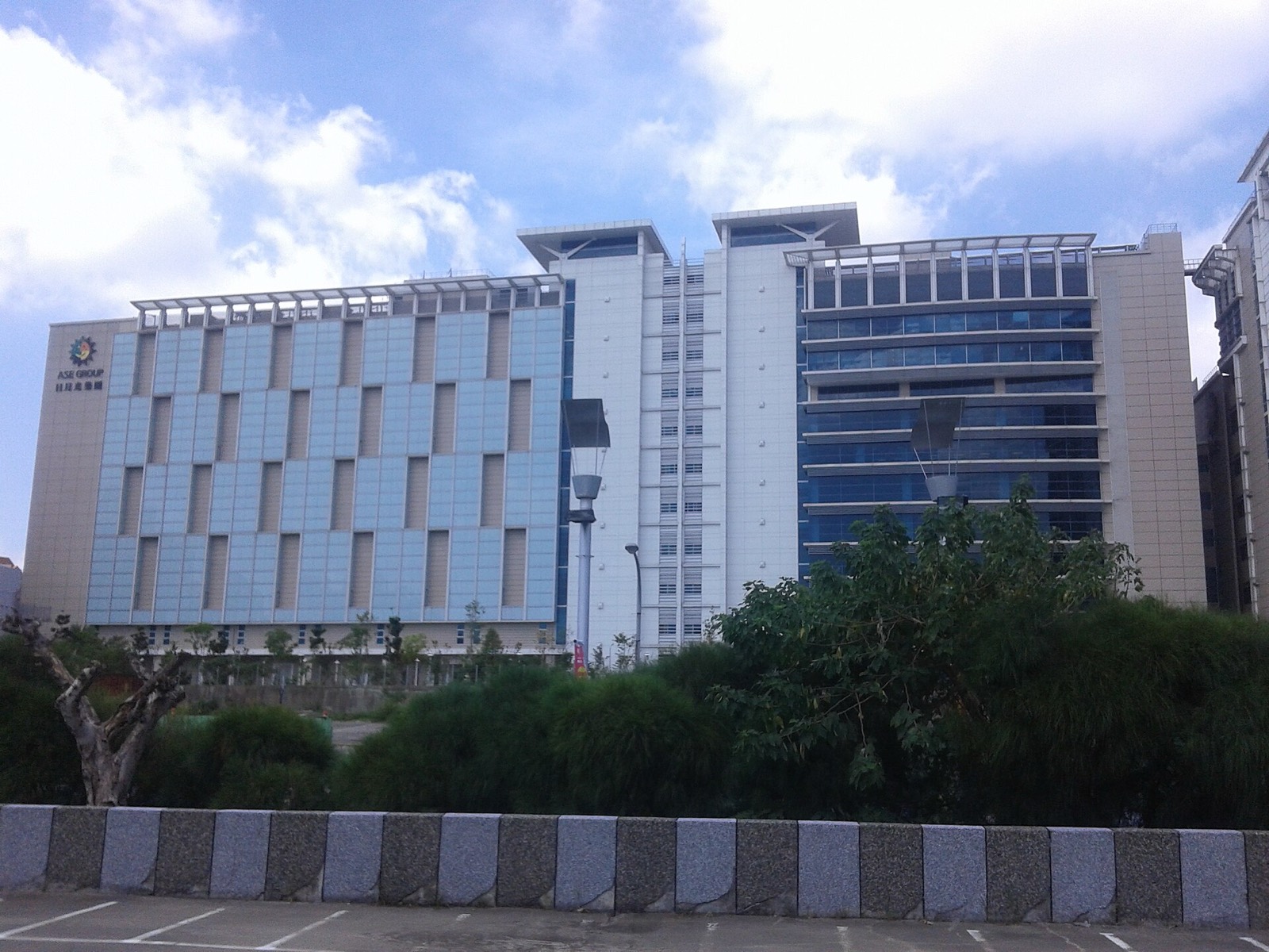 ASE Technology
The world's largest packaging and test house (OSAT).
AT
Amkor Technology
The US-headquartered OSAT building advanced packaging in Arizona.
GL
GlobalFoundries
The trailing-edge specialist that still fabricates Groq's LPU.
SM
SMIC
China's leading foundry, pushing 7 nm-class production without EUV.
ASE Technology
The world's largest packaging and test house (OSAT).
AT
Amkor Technology
The US-headquartered OSAT building advanced packaging in Arizona.
GL
GlobalFoundries
The trailing-edge specialist that still fabricates Groq's LPU.
SM
SMIC
China's leading foundry, pushing 7 nm-class production without EUV.
ASE Technology
The world's largest packaging and test house (OSAT).
AT
Amkor Technology
The US-headquartered OSAT building advanced packaging in Arizona.
GL
GlobalFoundries
The trailing-edge specialist that still fabricates Groq's LPU.
SM
SMIC
China's leading foundry, pushing 7 nm-class production without EUV.
Process nodes
6
TN
TSMC N5 / 4N (5 nm class)
The node of the AI era: Hopper, MI300, TPU v5, Maia all live here.
I1
Intel 18A
America's leading-edge hope: RibbonFET + backside power at Intel's fabs.
TN
TSMC N2 (2 nm)
Gate-all-around arrives: volume production from late 2025.
TN
TSMC N3 (3 nm)
The current leading edge in volume: MI355X, Trainium3, Rubin-class parts.
TN
TSMC N4P / 4NP
The refined 5 nm derivative under Blackwell.
TN
TSMC N7 (7 nm)
The 2018–20 node of A100, TPU v4 and the first AI boom.
Литография
2
EL
EUV Lithography
13.5-nanometer light from exploding tin droplets — the machine behind every leading-edge chip.
HN
High-NA EUV
The ~$380M next step: bigger optics, finer features, halved field size.
Advanced packaging
3
CO
CoWoS
TSMC's 2.5D packaging — the assembly step that rationed the world's GPUs.
E&
EMIB & Foveros
Intel's bridge-and-stack packaging arsenal.
S(
SoIC (3D Stacking)
TSMC's die-on-die hybrid bonding — true 3D chips.
Semiconductor equipment
7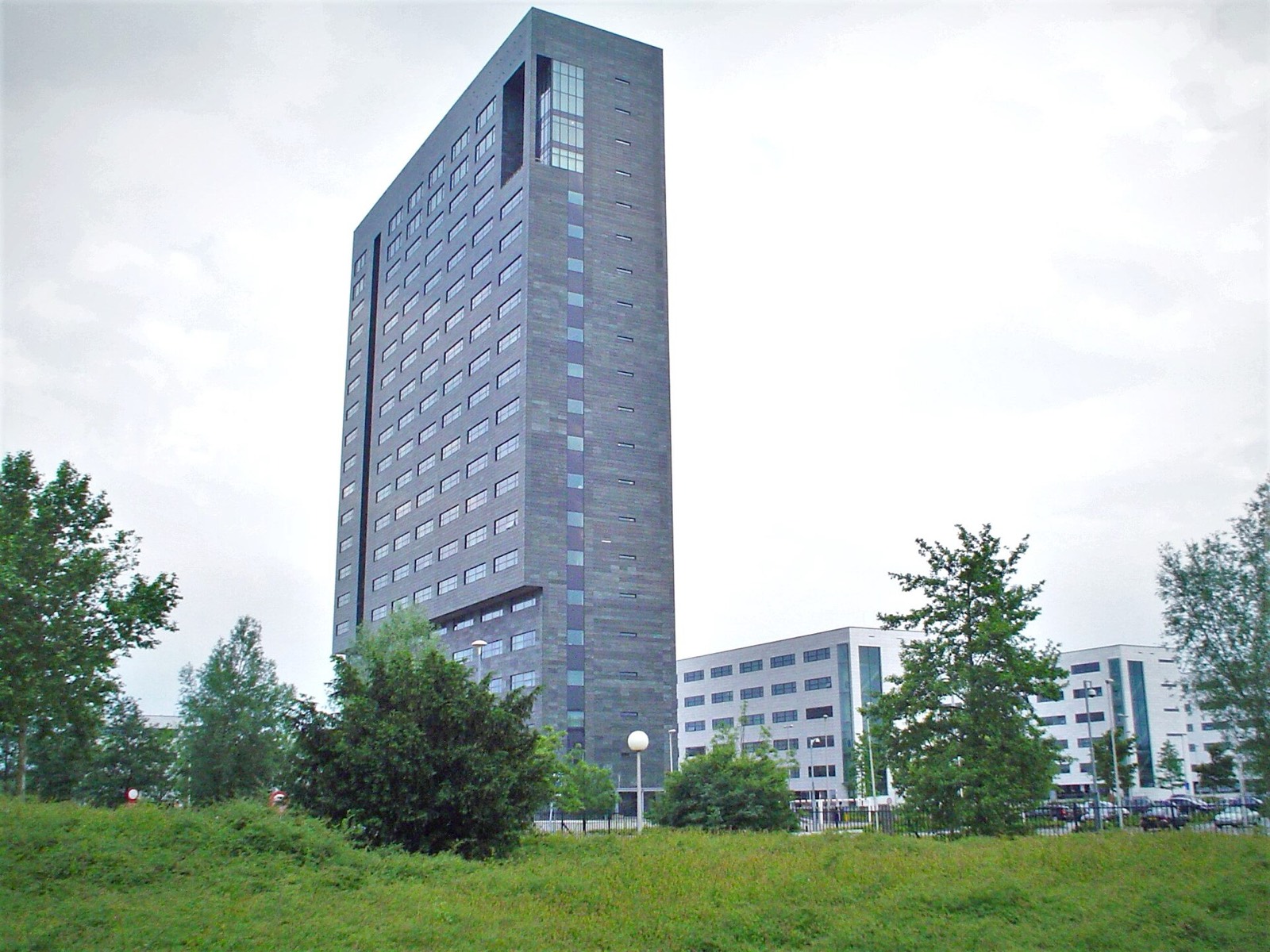 ASML
The only maker of EUV lithography machines — a literal monopoly at the source.
AM
Applied Materials
The broadest toolmaker: deposition, etch, implant — and packaging tools too.
BS
BE Semiconductor (Besi)
The hybrid-bonding specialist for the 3D-stacking era.
DC
DISCO Corporation
The company that cuts and grinds nearly every advanced chip.
KL
KLA
Process control: the inspection tools that make advanced yields possible.
LR
Lam Research
Etch and deposition leader — critical to HBM's through-silicon vias.
TE
Tokyo Electron
Japan's equipment giant — coaters, etchers and bonders in every fab.
ASML
The only maker of EUV lithography machines — a literal monopoly at the source.
AM
Applied Materials
The broadest toolmaker: deposition, etch, implant — and packaging tools too.
BS
BE Semiconductor (Besi)
The hybrid-bonding specialist for the 3D-stacking era.
DC
DISCO Corporation
The company that cuts and grinds nearly every advanced chip.
KL
KLA
Process control: the inspection tools that make advanced yields possible.
LR
Lam Research
Etch and deposition leader — critical to HBM's through-silicon vias.
TE
Tokyo Electron
Japan's equipment giant — coaters, etchers and bonders in every fab.