Datenbankbereich · 26 Datensätze
Foundries & Packaging
Where the chips are actually made: leading-edge process nodes, advanced packaging, and the equipment monopolies underneath.
Feldnotizen
Alles oberhalb dieser Schicht ist Design; in dieser Schicht werden tatsächlich Atome bewegt. Sie ist auch der konzentrierteste Ort in der Weltwirtschaft: Ein Unternehmen fertigt nahezu jeden fortschrittlichen KI-Chip – mit Maschinen, die nur ein einziges anderes Unternehmen bauen kann.
Mit diesen drei beginnen
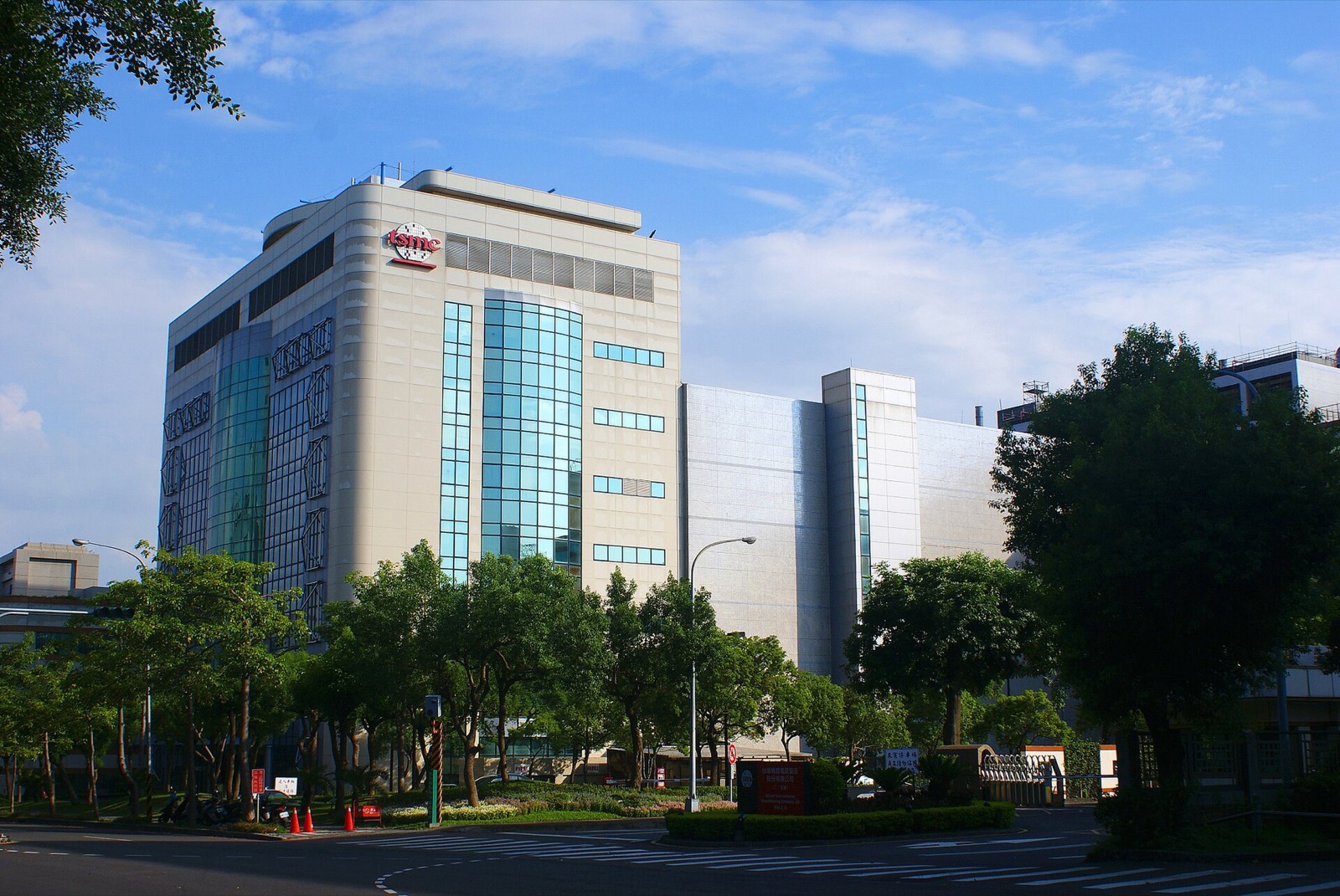 TSMC
Das unverzichtbare Unternehmen. Nahezu jeder Chip in dieser Datenbank wurde hier geboren.
EL
EUV Lithography
Die Maschine, die nur ASML bauen kann – Zinntröpfchen, Laser und die flachsten Spiegel, die je gefertigt wurden.
CO
CoWoS
Der Packaging-Schritt, der die weltweite GPU-Versorgung zwei Jahre lang rationierte.
TSMC
Das unverzichtbare Unternehmen. Nahezu jeder Chip in dieser Datenbank wurde hier geboren.
EL
EUV Lithography
Die Maschine, die nur ASML bauen kann – Zinntröpfchen, Laser und die flachsten Spiegel, die je gefertigt wurden.
CO
CoWoS
Der Packaging-Schritt, der die weltweite GPU-Versorgung zwei Jahre lang rationierte.
Foundries & packaging houses
5
TS
TSMC
The indispensable factory: nearly every leading AI chip is made here.
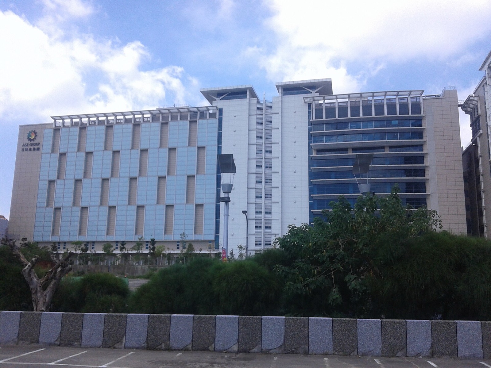 ASE Technology
The world's largest packaging and test house (OSAT).
AT
Amkor Technology
The US-headquartered OSAT building advanced packaging in Arizona.
GL
GlobalFoundries
The trailing-edge specialist that still fabricates Groq's LPU.
SM
SMIC
China's leading foundry, pushing 7 nm-class production without EUV.
ASE Technology
The world's largest packaging and test house (OSAT).
AT
Amkor Technology
The US-headquartered OSAT building advanced packaging in Arizona.
GL
GlobalFoundries
The trailing-edge specialist that still fabricates Groq's LPU.
SM
SMIC
China's leading foundry, pushing 7 nm-class production without EUV.
ASE Technology
The world's largest packaging and test house (OSAT).
AT
Amkor Technology
The US-headquartered OSAT building advanced packaging in Arizona.
GL
GlobalFoundries
The trailing-edge specialist that still fabricates Groq's LPU.
SM
SMIC
China's leading foundry, pushing 7 nm-class production without EUV.
Process nodes
6
TN
TSMC N5 / 4N (5 nm class)
The node of the AI era: Hopper, MI300, TPU v5, Maia all live here.
I1
Intel 18A
America's leading-edge hope: RibbonFET + backside power at Intel's fabs.
TN
TSMC N2 (2 nm)
Gate-all-around arrives: volume production from late 2025.
TN
TSMC N3 (3 nm)
The current leading edge in volume: MI355X, Trainium3, Rubin-class parts.
TN
TSMC N4P / 4NP
The refined 5 nm derivative under Blackwell.
TN
TSMC N7 (7 nm)
The 2018–20 node of A100, TPU v4 and the first AI boom.
Lithografie
2
EL
EUV Lithography
13.5-nanometer light from exploding tin droplets — the machine behind every leading-edge chip.
HN
High-NA EUV
The ~$380M next step: bigger optics, finer features, halved field size.
Advanced packaging
3
CO
CoWoS
TSMC's 2.5D packaging — the assembly step that rationed the world's GPUs.
E&
EMIB & Foveros
Intel's bridge-and-stack packaging arsenal.
S(
SoIC (3D Stacking)
TSMC's die-on-die hybrid bonding — true 3D chips.
Semiconductor equipment
7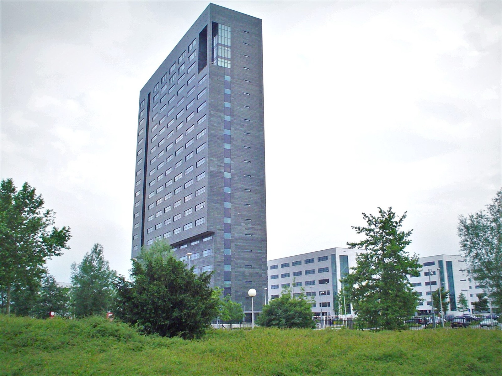 ASML
The only maker of EUV lithography machines — a literal monopoly at the source.
AM
Applied Materials
The broadest toolmaker: deposition, etch, implant — and packaging tools too.
BS
BE Semiconductor (Besi)
The hybrid-bonding specialist for the 3D-stacking era.
DC
DISCO Corporation
The company that cuts and grinds nearly every advanced chip.
KL
KLA
Process control: the inspection tools that make advanced yields possible.
LR
Lam Research
Etch and deposition leader — critical to HBM's through-silicon vias.
TE
Tokyo Electron
Japan's equipment giant — coaters, etchers and bonders in every fab.
ASML
The only maker of EUV lithography machines — a literal monopoly at the source.
AM
Applied Materials
The broadest toolmaker: deposition, etch, implant — and packaging tools too.
BS
BE Semiconductor (Besi)
The hybrid-bonding specialist for the 3D-stacking era.
DC
DISCO Corporation
The company that cuts and grinds nearly every advanced chip.
KL
KLA
Process control: the inspection tools that make advanced yields possible.
LR
Lam Research
Etch and deposition leader — critical to HBM's through-silicon vias.
TE
Tokyo Electron
Japan's equipment giant — coaters, etchers and bonders in every fab.