Ask why any given AI chip is fast, scarce or expensive and the answer is usually the same three letters: HBM.
The problem it solves
Generating one token means streaming essentially all of a model's active weights through the compute units. A 70B-parameter model at 8 bits is 70 GB per token — at 100 tokens/second, that is 7 TB/s of appetite. No memory on a motherboard gets close; the data must live millimeters from the die on the widest possible wires.
The solution: go vertical
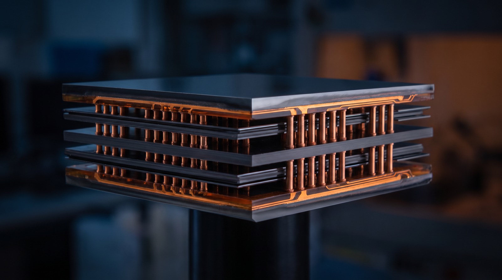
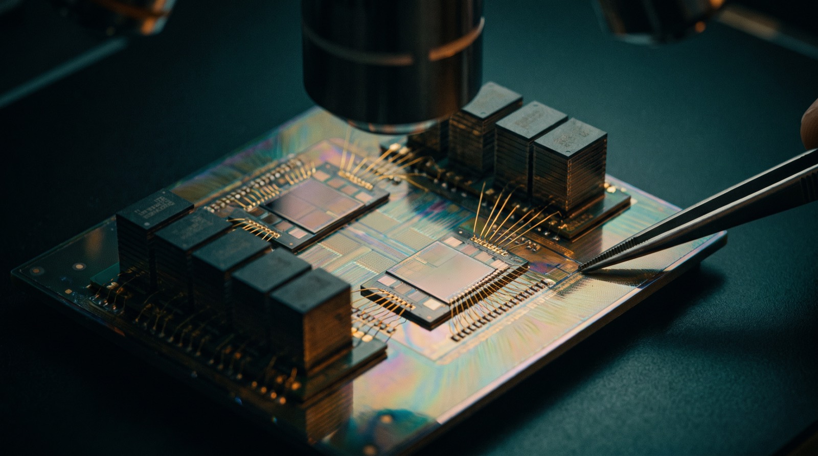
HBM stacks 8–12 DRAM dies, drills thousands of through-silicon vias down the stack, and mounts it beside the GPU on a silicon interposer. A single HBM3E stack moves ~1.2 TB/s over a 1,024-bit bus; eight stacks give the B200 its 8 TB/s. HBM4 (2026) doubles the bus to 2,048 bits and — a quiet revolution — puts a logic base die from a foundry under the stack, blurring memory into processor.
Three makers, sold out
Only SK hynix (the leader, ~half the market per TrendForce estimates), Samsung and Micron manufacture HBM, and all three have described output as effectively sold out about a year in advance through the boom. HBM yield is brutal — stack twelve dies and one bad die kills all twelve — and each generation must be qualified per-GPU, which is why Samsung's slow HBM3E qualification at NVIDIA was a global business story.
Reading the market through memory
Memory capacity per GPU is the cleanest tell of product strategy: H100's 80 GB → H200's 141 GB → B300's 288 GB → MI400's announced 432 GB. Chips win sockets on memory as much as FLOPS (MI300X's 192 GB won Azure serving), export controls now list HBM explicitly, and SK hynix's profits passing Samsung's semiconductor division in 2025 was the memory market's regime change in one headline. When you read our Trends page, HBM is the commodity behind half the stories.
 3
3