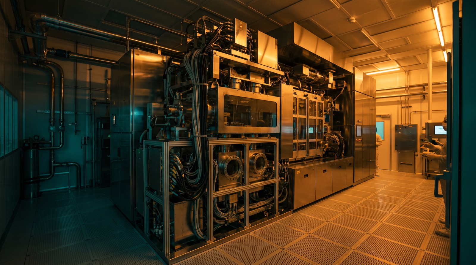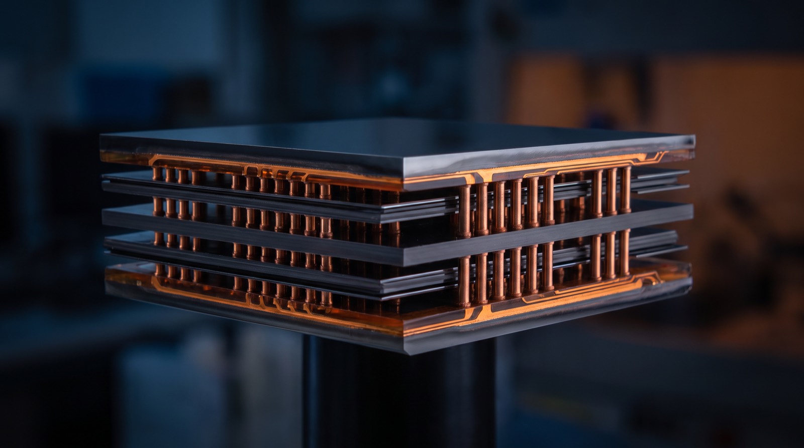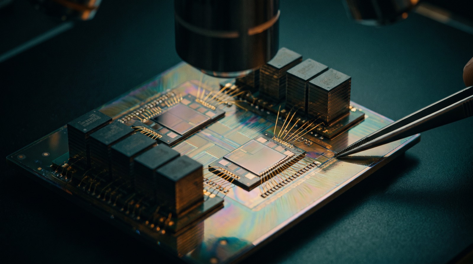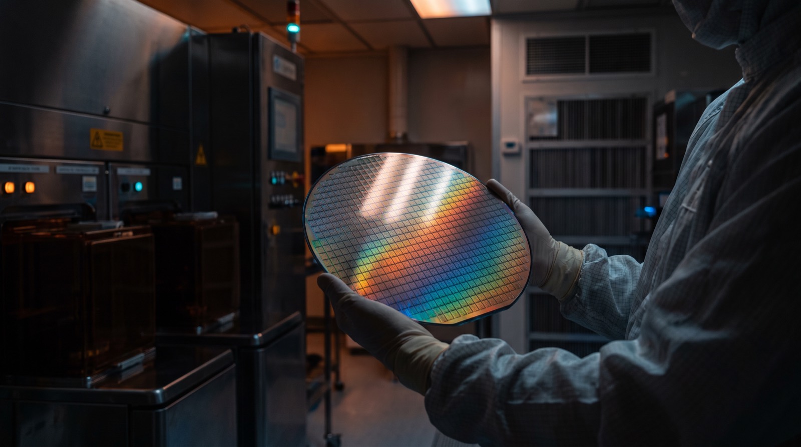
Every chip page in this database lists a process node — N7, N5, N3, 18A. The names lie a little; the differences are real.
The name is not a measurement
Since ~2010, node names stopped corresponding to any physical dimension. "3 nm" transistors have no 3 nm feature; the name means roughly "the generation after 5 nm, with ~1.6-1.7x the logic density." Compare nodes by what they deliver: transistors per mm², performance per watt, and cost per transistor (which, ominously, no longer always falls).
What a node buys an AI chip
Each full step gives roughly 25–40% better performance-per-watt or ~1.5x density. On a 1,000 W accelerator, that is the difference between fitting in a rack's power budget or not. MI355X on N3P packs 185B transistors; Blackwell stayed on a mature 4N variant and spent its innovation on packaging instead — both are valid strategies, and the contrast explains a lot of 2025's product texture.
The living roadmap
TSMC N2 (volume from late 2025) introduces gate-all-around nanosheet transistors; A16 (late 2026) adds backside power delivery — moving power wiring under the transistors, a big deal for power-hungry AI dies. Intel 18A shipped backside power first and is Intel's bid to matter again; Samsung fights for relevance at 2 nm with Tesla's AI6 as its marquee win. SMIC, denied EUV, pushes 7 nm-class DUV multi-patterning for Huawei at painful cost — the clearest measure of what export controls actually do.
How to use this knowledge
When a chip record here says "TSMC N5, 2022," you can infer its density class, its power class, and its place in the queue for capacity. And when vendors announce 2026–27 parts, the first question is always the same: whose node, and who else is in line for it.