Google TPU v1–v3
The originals: the 2015 inference ASIC that started the custom-silicon era.
您正在查看一条芯片记录:该处理器是什么、其关键规格、谁设计它、谁制造它、谁供应其零部件,以及它被用在哪里。
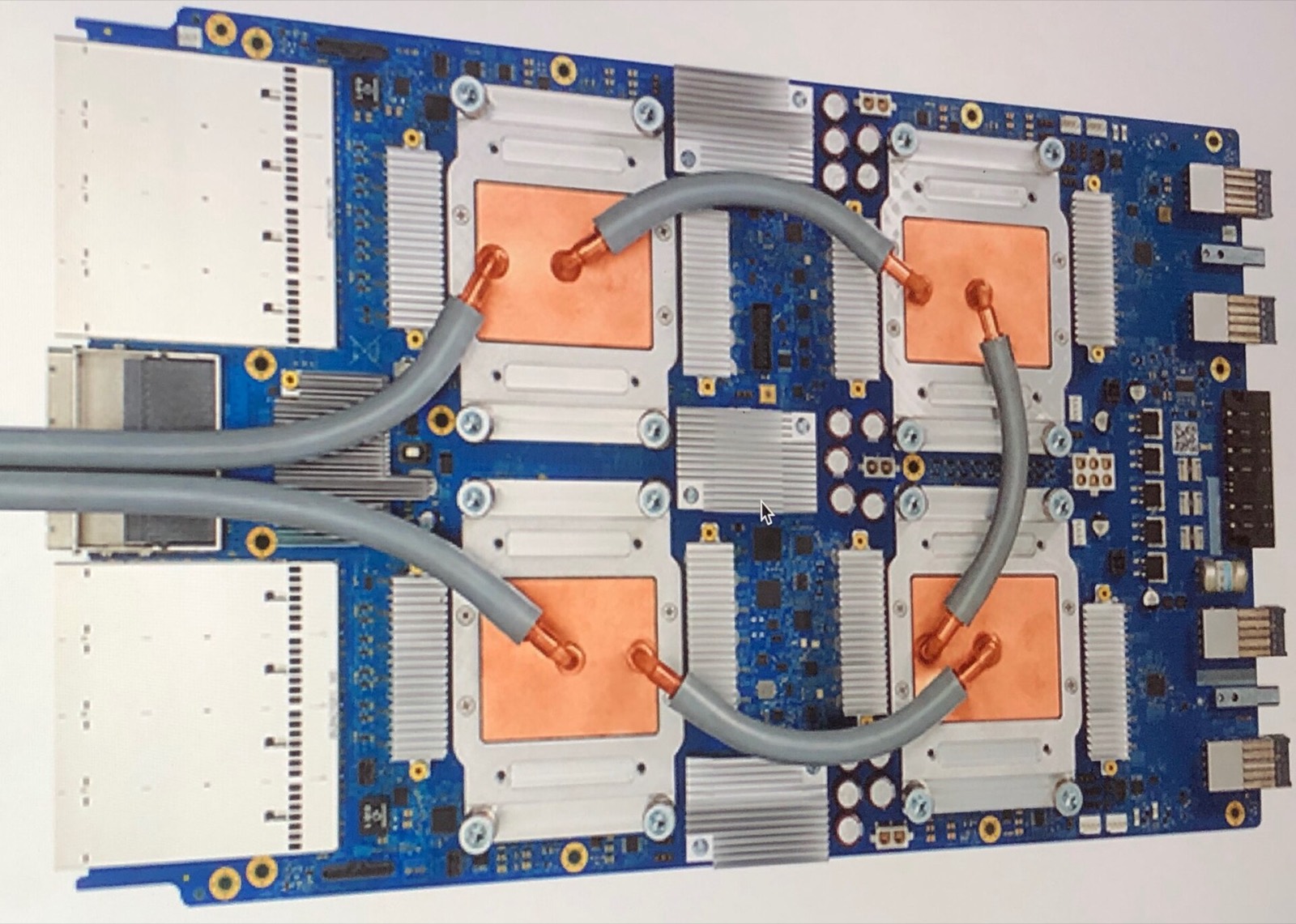
照片: Zinskauf · CC BY-SA 4.0 · Wikimedia Commons
TPU v1 (deployed 2015, revealed 2016) was a 28 nm inference ASIC built in 15 months after Google calculated that voice search at scale would otherwise require doubling its data centers. v2 (2017) added training, HBM and the first pods; v3 (2018) went liquid-cooled at 1,024-chip scale and trained early BERT-era models. Together they proved a hyperscaler could out-build the merchant market for its own workloads — the argument every custom AI chip since has followed. AlphaGo ran on TPUs when it beat Lee Sedol in 2016.
规格与关键参数
每个数据均标注来源依据:厂商规格、厂商声明、公开报道、估算或官方数据。"未公开披露"即字面含义——我们从不捏造数值。
Overview
算力
它如何与整个技术栈相连
本记录的关联链接一览——点击分组可直接跳转。
用于训练
后继产品
来源
记录审阅截至 2026-01-15 — 查看 方法论.