Google TPU v1–v3
The originals: the 2015 inference ASIC that started the custom-silicon era.
현재 보고 계신 것은 칩 레코드입니다: 이 프로세서가 무엇인지, 주요 사양, 설계·제조·부품 공급사, 그리고 어디에 활용되는지를 다룹니다.
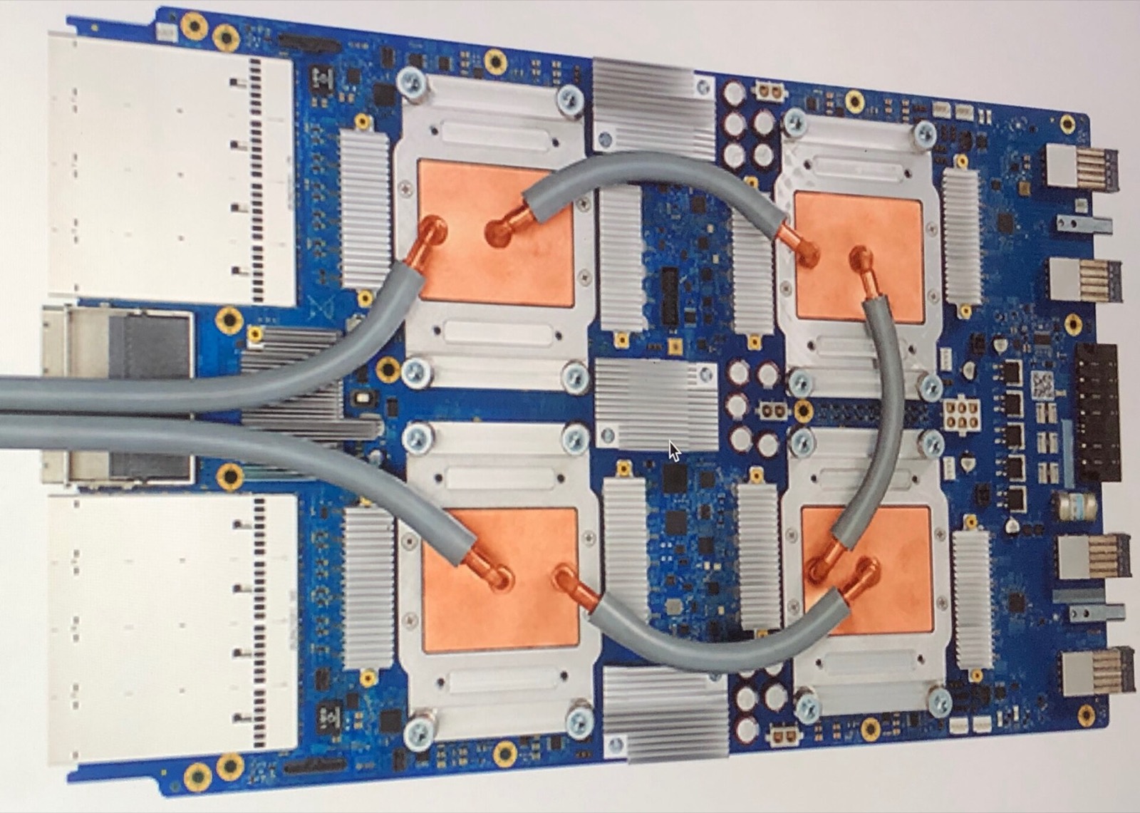
사진: Zinskauf · CC BY-SA 4.0 · Wikimedia Commons
TPU v1 (deployed 2015, revealed 2016) was a 28 nm inference ASIC built in 15 months after Google calculated that voice search at scale would otherwise require doubling its data centers. v2 (2017) added training, HBM and the first pods; v3 (2018) went liquid-cooled at 1,024-chip scale and trained early BERT-era models. Together they proved a hyperscaler could out-build the merchant market for its own workloads — the argument every custom AI chip since has followed. AlphaGo ran on TPUs when it beat Lee Sedol in 2016.
사양 및 주요 정보
각 수치에는 근거 유형이 표시됩니다: 벤더 사양, 벤더 주장, 보고된 값, 추정치, 또는 공식 발표. "공개되지 않음"은 그대로의 의미이며, 값을 임의로 만들어내는 일은 없습니다.
Overview
컴퓨트
전체 스택에서의 연결 구조
이 레코드의 링크를 한눈에 확인하세요 — 그룹을 클릭하면 해당 위치로 이동합니다.
학습에 사용됨
후속 제품
출처
검토 기준일 2026-01-15 — 보기 방법론.