Google TPU v1–v3
The originals: the 2015 inference ASIC that started the custom-silicon era.
これはチップのレコードです。このプロセッサの概要、主要スペック、設計・製造・部品供給を担う企業、および用途を紹介します。
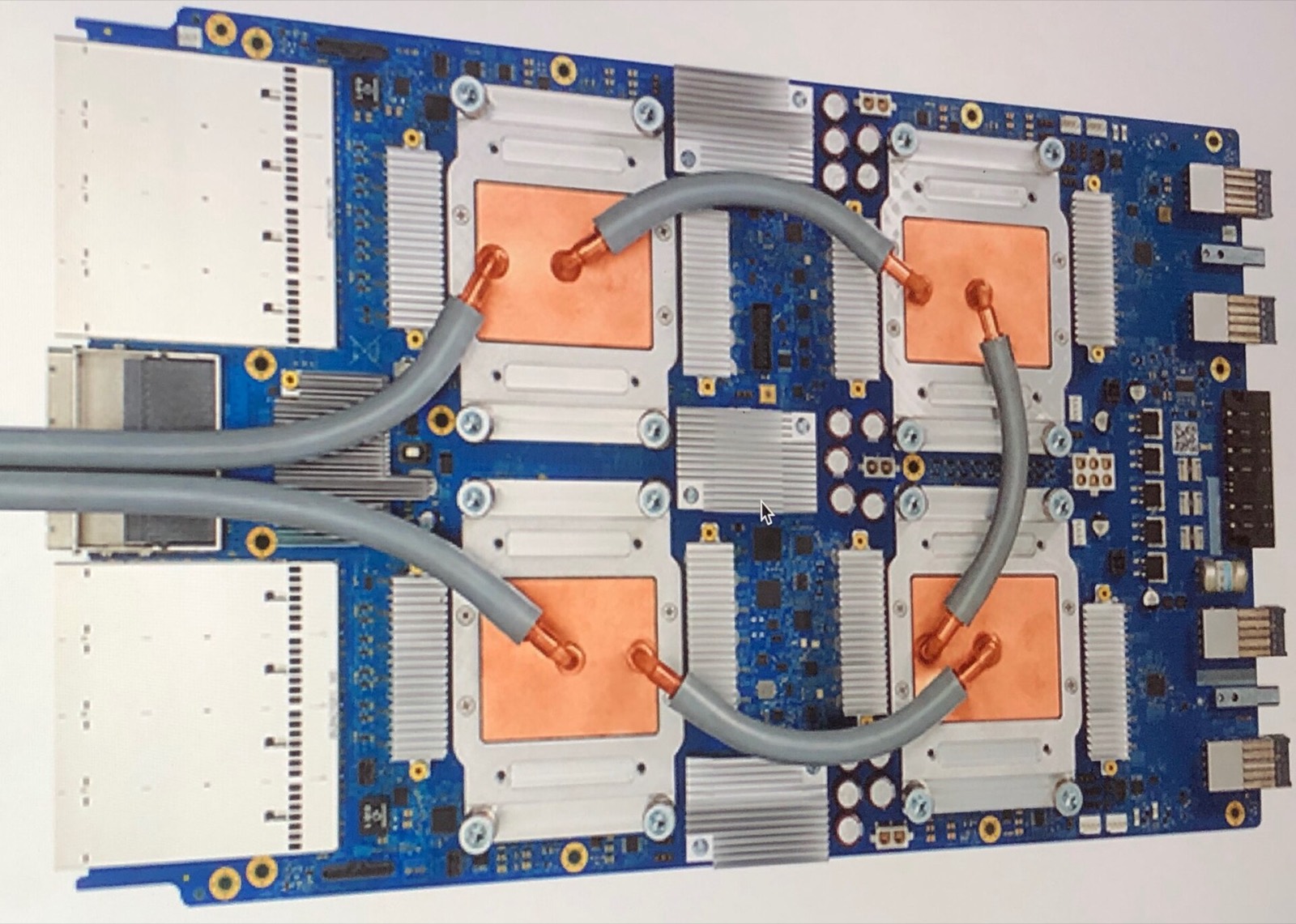
写真: Zinskauf · CC BY-SA 4.0 · Wikimedia Commons
TPU v1 (deployed 2015, revealed 2016) was a 28 nm inference ASIC built in 15 months after Google calculated that voice search at scale would otherwise require doubling its data centers. v2 (2017) added training, HBM and the first pods; v3 (2018) went liquid-cooled at 1,024-chip scale and trained early BERT-era models. Together they proved a hyperscaler could out-build the merchant market for its own workloads — the argument every custom AI chip since has followed. AlphaGo ran on TPUs when it beat Lee Sedol in 2016.
仕様・主要事実
各数値には根拠の種別を明記しています:ベンダー仕様、ベンダー主張、報道値、推定値、または公式値。「非公開」とある場合はその通りであり、当サイトが値を創作することは一切ありません。
Overview
コンピュート
スタック全体とのつながり
このレコードのリンク一覧 — グループをクリックするとジャンプします。
学習に使用
後継製品
出典
レコードのレビュー時点: 2026-01-15 — 表示 調査手法.