★
Menu
Home How It's Built Watchlist The Stack
Hardware ChipsCompare Chips Servers & SystemsNetworking MemoryFoundries & Packaging Cooling
Facilities Data CentersPower ProjectsCloud & GPU Compute
Intelligence AI ModelsSoftware AI ProductsBenchmarks Research PapersDatasets Concepts
Ecosystem CompaniesStocks PeopleTimeline TrendsFuture of AI
Learn News Ask the Data AI Agents
About About us Methodology Data & API Disclaimer
Options
DATA & API

Free read-only JSON access to the site's cached data.

Dark mode

Guided View
New to chips, data centers and model jargon? We explain key terms as you browse, in plain English. Same data, with the help built in.

Expert View
You already know the stack. Just the data: clean, fast and compact, with no extra explanations. This is the default view.

Interface language
‹ Back
Home › Chips › Google TPU v1–v3

Google TPU v1–v3

Chip AI Accelerator Historical

The originals: the 2015 inference ASIC that started the custom-silicon era.

You're looking at a chip record: what this processor is, its key specs, who designs, manufactures and supplies its parts, and where it gets used.
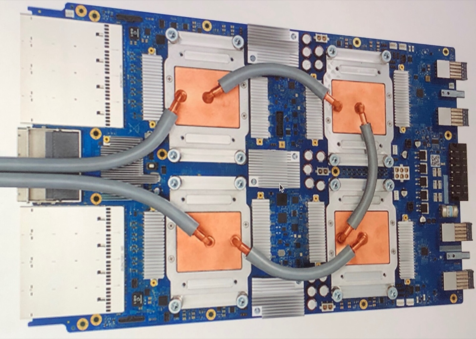
Photo: Zinskauf · CC BY-SA 4.0 · Wikimedia Commons

TPU v1 (deployed 2015, revealed 2016) was a 28 nm inference ASIC built in 15 months after Google calculated that voice search at scale would otherwise require doubling its data centers. v2 (2017) added training, HBM and the first pods; v3 (2018) went liquid-cooled at 1,024-chip scale and trained early BERT-era models. Together they proved a hyperscaler could out-build the merchant market for its own workloads — the argument every custom AI chip since has followed. AlphaGo ran on TPUs when it beat Lee Sedol in 2016.

Specifications & key facts

Each figure is labeled by basis: vendor spec, vendor claim, reported, estimate, or official. "Not publicly disclosed" means exactly that — we never invent values.

Overview

Designer Google
Deployed v1 2015 · v2 2017 · v3 2018
Legacy Introduced BF16 to hardware and the pod-scale systems model

Compute

TPU v1 92 TOPS INT8, inference onlyPublished paper
TPU v2 45 TFLOPS BF16 per chip; first 256-chip podsVendor spec
TPU v3 123 TFLOPS BF16 per chip; liquid-cooled 1,024-chip podsVendor spec

How this connects to the rest of the stack

This record's links at a glance — click a group to jump to it.

Designed by

Used to train

Succeeded by

Sources

TPU v1 paper (ISCA 2017) ↗

Record reviewed as of 2026-01-15 — see Methodology.